


Gallium Arsenide
GaAs
Gallium Arsenide GaAsAng mga wafer kasagarang gigamit sa paghimo sa mga elektronikong himan sama sa infrared light-emitting diodes, laser diodes, optical windows, field-effect transistors FETs, linear sa digital ICs ug solar cells.Ang mga component sa GaAs mapuslanon sa ultra-high radio frequency ug paspas nga electronic switching application, weak-signal amplification applications.Dugang pa, ang substrate sa Gallium Arsenide usa ka sulundon nga materyal alang sa paghimo sa mga sangkap sa RF, frequency sa microwave ug monolithic ICs, ug mga aparato sa LED sa mga optical nga komunikasyon ug mga sistema sa pagkontrol alang sa paglihok sa saturated hall, taas nga gahum ug kalig-on sa temperatura.
| Dili. | Mga butang | Standard nga Espesipikasyon | |||
| 1 | Gidak-on | 2" | 3" | 4" | 6" |
| 2 | Diametro mm | 50.8±0.3 | 76.2±0.3 | 100±0.5 | 150±0.5 |
| 3 | Pamaagi sa Pagtubo | VGF | VGF | VGF | VGF |
| 4 | Uri sa Conductivity | N-Type/Si o Te-doped, P-Type/Zn-doped, Semi-Insulating/Un-doped | |||
| 5 | Oryentasyon | (100)±0.5° | (100)±0.5° | (100)±0.5° | (100)±0.5° |
| 6 | Gibag-on μm | 350±25 | 625±25 | 625±25 | 650±25 |
| 7 | Patag nga orientasyon mm | 17±1 | 22±1 | 32±1 | Notch |
| 8 | Identification Flat mm | 7±1 | 12±1 | 18±1 | - |
| 9 | Resistivity Ω-cm | (1-9)E(-3) para sa p-type o n-type, (1-10)E8 para sa semi-insulating | |||
| 10 | Paglihok cm2/vs | 50-120 para sa p-type, (1-2.5)E3 para sa n-type, ≥4000 para sa semi-insulating | |||
| 11 | Konsentrasyon sa Tagdala cm-3 | (5-50)E18 para sa p-type, (0.8-4)E18 para sa n-type | |||
| 12 | TTV μm max | 10 | 10 | 10 | 10 |
| 13 | Bow μm max | 30 | 30 | 30 | 30 |
| 14 | Warp μm max | 30 | 30 | 30 | 30 |
| 15 | EPD cm-2 | 5000 | 5000 | 5000 | 5000 |
| 16 | Paghuman sa nawong | P/E, P/P | P/E, P/P | P/E, P/P | P/E, P/P |
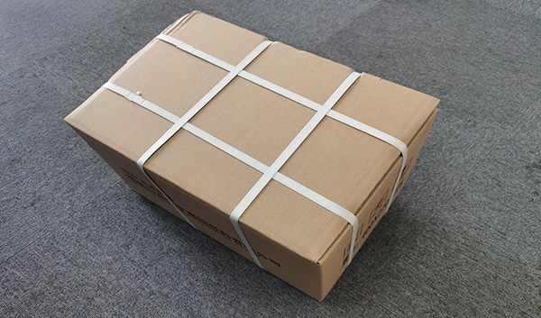
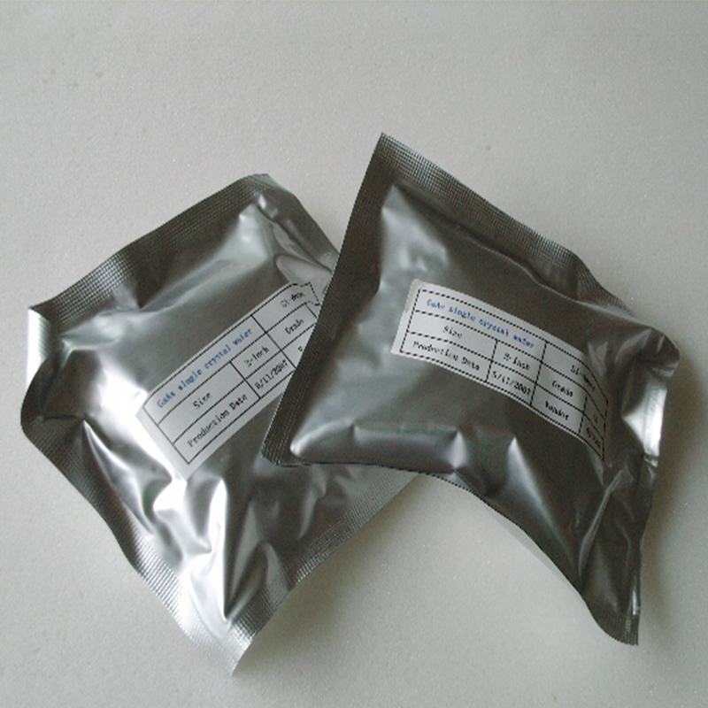
| 17 | Pagputos | Usa ka wafer nga sudlanan nga gisilyohan sa aluminum composite bag. | |||
| 18 | Mga komento | Ang mekanikal nga grado nga GaAs wafer magamit usab kung gihangyo. | |||
| Linear nga Pormula | GaAs |
| Molekular nga Timbang | 144.64 |
| Kristal nga istruktura | Pagsagol sa zinc |
| Panagway | Gray nga kristal nga solid |
| Punto sa Pagkatunaw | 1400°C, 2550°F |
| Nagbukal nga Punto | N/A |
| Densidad sa 300K | 5.32 g/cm3 |
| Gap sa Enerhiya | 1.424 eV |
| Intrinsic nga resistivity | 3.3E8 Ω-cm |
| Numero sa CAS | 1303-00-0 |
| Numero sa EC | 215-114-8 |
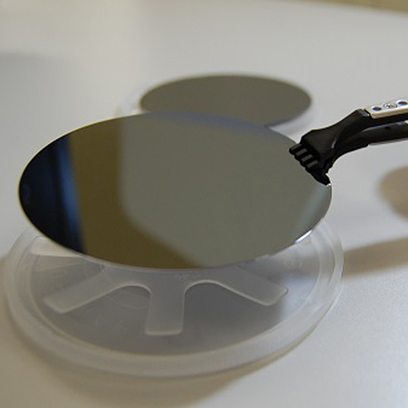
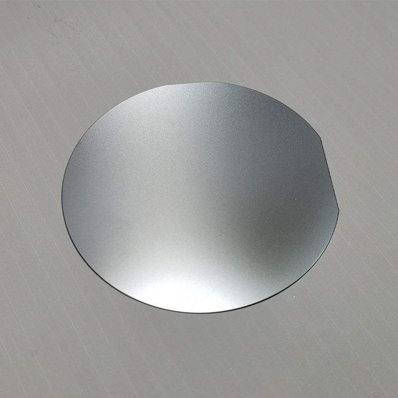
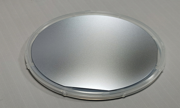
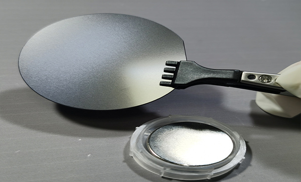
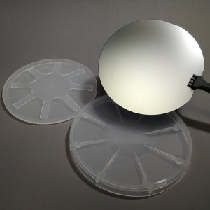
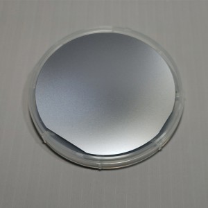
Gallium Arsenide GaAssa Western Minmetals (SC) Corporation mahimong ma-supply isip polycrystalline lump o single crystal wafer sa as-cut, etched, polished, o epi-ready nga mga wafer sa gidak-on nga 2" 3" 4" ug 6" (50mm, 75mm, 100mm , 150mm) diametro, nga adunay p-type, n-type o semi-insulating conductivity, ug <111> o <100> orientation.Ang gipahiangay nga detalye alang sa hingpit nga solusyon sa among mga kostumer sa tibuuk kalibutan.


- Sample Anaa Sa Paghangyo
- Kaluwasan nga Paghatud sa mga Butang Pinaagi sa Courier/Air/Sea
- Pagdumala sa Kalidad sa COA/COC
- Luwas ug Sayon nga Pagputos
- UN Standard Packing Anaa Sa Paghangyo
- ISO9001:2015 Certified
- Mga Termino sa CPT/CIP/FOB/CFR Pinaagi sa Incoterms 2010
- Flexible nga Termino sa Pagbayad T/TD/PL/C Madawat
- Bug-os nga Dimensyon nga After-Sale nga Serbisyo
- Quality Inspection Pinaagi sa Sate-of-the-art nga Pasilidad
- Pag-apruba sa mga Regulasyon sa Rohs/REACH
- Non-Disclosure Agreements NDA
- Non-Conflict Mineral Policy
- Regular nga Pagrepaso sa Pagdumala sa Kalikopan
- Katumanan sa Social Responsibility


- English
- French
- German
- Portuguese
- Spanish
- Russian
- Japanese
- Korean
- Arabic
- Irish
- Greek
- Turkish
- Italian
- Danish
- Romanian
- Indonesian
- Czech
- Afrikaans
- Swedish
- Polish
- Basque
- Catalan
- Esperanto
- Hindi
- Lao
- Albanian
- Amharic
- Armenian
- Azerbaijani
- Belarusian
- Bengali
- Bosnian
- Bulgarian
- Cebuano
- Chichewa
- Corsican
- Croatian
- Dutch
- Estonian
- Filipino
- Finnish
- Frisian
- Galician
- Georgian
- Gujarati
- Haitian
- Hausa
- Hawaiian
- Hebrew
- Hmong
- Hungarian
- Icelandic
- Igbo
- Javanese
- Kannada
- Kazakh
- Khmer
- Kurdish
- Kyrgyz
- Latin
- Latvian
- Lithuanian
- Luxembou..
- Macedonian
- Malagasy
- Malay
- Malayalam
- Maltese
- Maori
- Marathi
- Mongolian
- Burmese
- Nepali
- Norwegian
- Pashto
- Persian
- Punjabi
- Serbian
- Sesotho
- Sinhala
- Slovak
- Slovenian
- Somali
- Samoan
- Scots Gaelic
- Shona
- Sindhi
- Sundanese
- Swahili
- Tajik
- Tamil
- Telugu
- Thai
- Ukrainian
- Urdu
- Uzbek
- Vietnamese
- Welsh
- Xhosa
- Yiddish
- Yoruba
- Zulu